- Sandisk says that 3D matrix memory will be an affordable replacement for DRAM
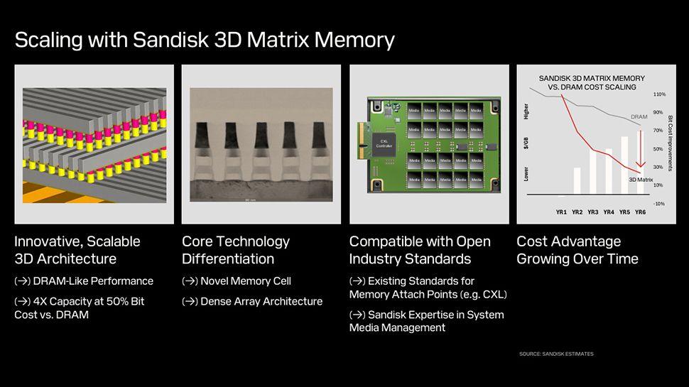
- Will offer DRAM type performance to 4x the capacity and half of the cost
- Sandisk says that he will become more affordable as technology matures
During its recent Sandisk 2.0 Investor Day session, the Flash storage giant unveiled a series of new SSDs, including a 128 TB data center model, while describing its ambitious roadmap for even larger readers – An SSD of 256 TB in 2026, an SSD of 512 TB in 2027, and a huge 1PB training expected a few years later.
Sandisk wants to calm any oscillation of investors after its separation from Western Digital, and beyond discuss its strategy to increase yields and margins, the company has also taken the wraps in its revolutionary 3D matrix memory, a technology evolving memory that would promise DRAM type performance four times the capacity and half of the cost.
Sandisk positioned 3D matrix memory as an affordable solution in response to the end of Moore’s law for the DRAM, where the stagnation of the scale, a difference in widening of the computing memory and the costs of the memory are become major challenges. Society affirms that its evolutionary memory architecture will cross the “wall of memory”, solving the problem of the ability of memory and the bandwidth of evil to keep the pace of ever -increasing processing requests.
More profitable
Developed in collaboration with IMEC, the 3D matrix memory of Sandisk is built on a dense network architecture with a new design of memory cells while maintaining compatibility with open industry standards, such as CXL.
The company says its new memory technology will become more and more profitable over time. According to a shared Sankisk graph by the 6th year, 3D matrix memory will achieve more than 50% of cost savings per bit compared to DRAM, with a significantly higher drop of $ / GB, making it an alternative more affordable to traditional dram solutions.
The company’s development roadmap, below, describes a certain number of milestones, with a transition from a 150 mm WD research fab to a 300 mm IMEC installation in 2024, marking the first significant step From technology to large -scale production.
From 2017, the project went from isolated devices to passive networks, CMOS development vehicles. Gen1 media samples will be the next big step and they should reach the capabilities 32-64 Gbit, although there are not yet details on raw performance.