- Kioxia develops high-density 3D DRAM using stackable oxide-semiconductor transistors
- Eight-layer transistor stacks demonstrate reliable operation in laboratory demonstrations
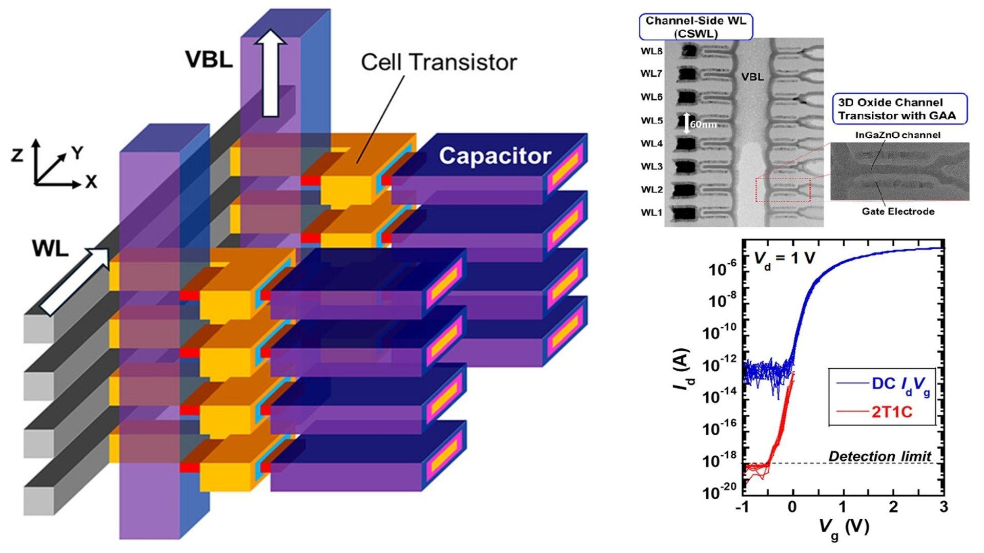
- Oxide semiconductor InGaZnO replaces silicon nitride for the formation of vertical and horizontal transistors
Kioxia claims to have developed highly stackable oxide-semiconductor channel transistors capable of supporting high-density 3D DRAM.
This development could lead to cheaper and faster memory by reducing manufacturing costs per gigabyte and improving energy efficiency through high on-current and ultra-low off-current transistors.
However, this technology requires precise multi-layer alignment, integration into standard manufacturing, and long-term reliability testing, which can take decades.
Innovations in transistor design
Presented at the recent IEEE International Electronic Devices Meeting in San Francisco, the technology demonstrated the operation of transistors stacked in eight vertical layers.
The vertical layers consist of horizontally aligned transistors formed by replacing conventional silicon nitride regions with an oxide-semiconductor material, InGaZnO.
This arrangement makes it possible to increase memory capacity without resorting to conventional planar DRAM structures.
Oxide-semiconductor channel transistors combine mature silicon oxide and silicon nitride films with the new material InGaZnO.
The 3D memory cell structure introduced by Kioxia adapts the vertical pitch, allowing more memory cells to be stacked per unit volume.
The horizontal transistors formed during this process exhibit a high on-current exceeding 30 microamps.
It also features an ultra-low cutoff current of less than 1 attoamp, minimizing power consumption during refresh cycles.
By reducing refresh power, the design addresses a major limitation of traditional DRAM, where power consumption increases with higher memory densities.
Replacing monocrystalline silicon with oxide semiconductors reduces both manufacturing complexity and energy requirements.
These improvements reduce the cost of manufacturing DRAM per gigabyte, although retail prices for end users are not expected to decrease in the near term.
The stacked transistor approach also targets applications that require high memory density with low power consumption, such as AI servers and IoT devices.
The improved efficiency could support processing larger data sets without the same proportional increase in power demand seen in conventional DRAM systems.
Despite these technical advances, the technological transition from laboratory demonstrations to mass production presents significant challenges.
Precisely aligning multiple layers, integrating oxide-semiconductor materials into standard production lines, and ensuring long-term reliability remain obstacles to commercialization.
The company plans to continue research and development to enable the practical implementation of 3D DRAM in real-world applications.
Although the technology has clear technical advantages in terms of energy efficiency, density and manufacturing feasibility, it will likely not reach consumer markets until the next decade.
That said, cheaper manufacturing per gigabyte does not guarantee lower retail prices, and widespread adoption will require overcoming both production and supply chain issues.
Via TechPowerUp
Follow TechRadar on Google News And add us as your favorite source to get our news, reviews and expert opinions in your feeds. Make sure to click the Follow button!
And of course you can too follow TechRadar on TikTok for news, reviews, unboxings in video form and receive regular updates from us on WhatsApp Also.