- IMEC researchers have found a way to grow lasers directly on silicon
- IMEC lasers use Gallium arseniure, a material that does not naturally bind with silicon
- This breakthrough could reduce costs and improve photonic fleas for AI and telecommunications
Silicon Photonics uses light to transmit data instead of relying on electrical signals, but as silicon itself cannot effectively generate light, it requires lasers as a light source.
Placing lasers on fleas has been traditionally a challenge because silicon – a material commonly found in the sand – is not suitable for the manufacture of lasers, and the best laser materials, such as Gallium (GAAS), do not work naturally with it. Existing methods need to link these materials to silicon, a process that is both expensive and useless.
Scientists from the Belgium Research Center IMEC, have found a solution to this problem which implies the growth of lasers directly on silicon. This discovery could lead to more affordable and scalable photonic devices, potentially transforming applications into data communication, automatic learning and AI.
Short wavelengths
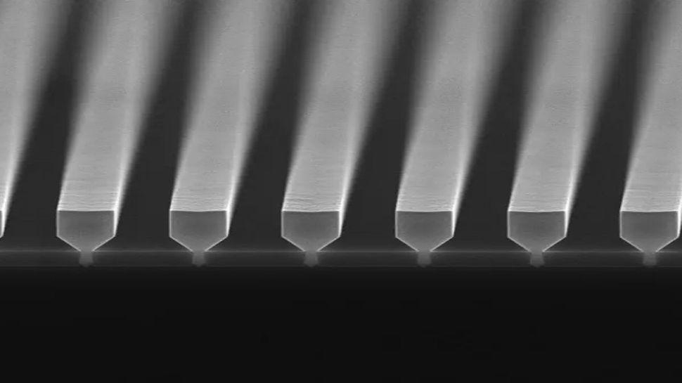
IMEC’s approach, detailed in an article published in NatureBases on nano -rid engineering, which limits the defects which would otherwise degrade the performance of the laser.
They start by covering a slice of silicon with a layer of silicon dioxide and engraving in the arrow -shaped trenches (“like a plowed field before planting” as Spectrum ieee Describes it). Gallium arseniure is then deposited in these trenches, where it is only in contact with silicon at the bottom. This placement maintains the defects buried in the trench and prevents them from spreading in the laser material above.
Lasers use multiple quantum wells of Gallium Arseniure (Ingaas) as a optical gain region and are integrated into a doped pins diode structure. They operate at room temperature with continuous wave -wave injection, reaching thresholds as low as 5 mA and output powers up to 1.75 MW.
“In recent years, the IMEC has been the pioneer of Nano-Rridge Engineering, a technique that is based on sagging [selective-area growth] and art [aspect-ratio trapping] To develop nano-Rridges with low defectivity III-V outside the trenches, “said Bernardette Kunert, scientific director of the IMEC.
“Now IMEC has exploited the concept of engineering III-V Nano-Rridge to demonstrate the first complete manufacturing on the scale of the lasers brochure based on electrically GAAS on standard 300 mm standard silicon plates, entirely in a CMOS pilot manufacturing line. “
Nanoridge lasers emit light to 1,020 nanometers, which Spectrum ieee Underline, is a shorter wavelength than those generally used in telecommunications. IMEC researchers say they are actively working to prolong the wavelength and improve design to reduce defects near electrical contacts. In case of success, this approach could provide an evolutionary and profitable solution to integrate lasers into silicon photonics, opening the way to high performance optical devices of the future.