- TDK spin photos detector pushes data speeds on AI ten times beyond today technology
- AI strange bottles can disappear while TDK trips are concentrated from GPU to data transfer
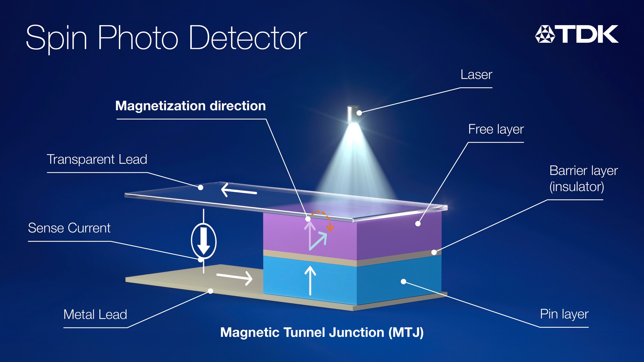
- Spin Photo Detector uses magnetism induced by laser for ultra-fast photoelectric conversion
The Japanese manufacturer TDK said that he had a major breakthrough in solving one of the most urgent problems of artificial intelligence. No, not GPU’s performance, but rather data transfer.
Its innovation, called the spin photos detector, combines magnetic, optical and electronic technologies to move data at speeds up to ten times faster than photodetectors based on existing semiconductors can offer.
The TDK device reaches response speeds of only 20 picoseconds – or $ 20 billion in seconds – using the light at a wavelength of 800 nanometers.
TDK spin photo detector
“This data transfer is the largest bottleneck for AI rather than the performance of semiconductor GPUs,” said Hideaki Fukuzawa, principal director of the company’s new generation product development center.
“Since we can unravel many of the current bottlenecks, we believe that this technology will change the situation for the AI and data center.”
To achieve this, TDK has re-commissioned its magnetic tunnel junction technology (MTJ), previously used in billions of hard drive heads.
The MTJ structure is only 200 nanometers wide and incorporates a single free layer of Cofeb which responds to laser pulses. It makes it possible to pass magnetic states parallel to antiparallels with 100% reliability under defined conditions.
Unlike the semiconductors that are based on the generation of carriers and the limits of the face to short wavelengths, spin photo detectors use electronic heating, allowing faster speeds and wider spectral coverage. MTJ elements are also resistant to cosmic rays, which makes them ideal for aerospace applications.
“Spin’s photos detector is a remarkable promise, both from a scientific and technological point of view,” said Arata Tsukamoto, professor of electrical engineering at Nihon University who collaborated with TDK on validation.
The TDK device has demonstrated effective operation on a wide range of wavelengths, from 300 Nm to 1.6 µm. Its ultra-fast analog light detection capacity, its energy efficiency and its compact size open up potential applications in AR / VR intelligent glasses, high-speed imagery and space systems. This development could also help solve energy consumption problems in the deployment of AI.
Technology could serve markets where fast and low latency data transfer is crucial for AI and graphic tasks.
TDK plans to provide samples by March 2026 and aims for mass production within five years. Thanks to the few stages of treatment required, it plans to maintain an advantage of costs and to challenge large flea manufacturers like TSMC and NVIDIA, who invest strongly in silicon photonics.
Via financial times