- WeeBit ReRAM memory integrates into chips without modifying existing transistor structures
- Each ReRAM cell stores data using resistive switching and not traditional flash methods
- ReRAM can handle between 100,000 and 1 million write cycles
Texas Instruments’ decision to license embedded ReRAM to Weebit Nano has reignited claims that flash memory has reached its structural limits.
The deal follows previous agreements with SkyWater, DB HiTek and Onsemi, marking a steady escalation in the number of manufacturing partners rather than an abrupt approval.
Weebit CEO Coby Hanoch said Everything about the circuits that the progression was deliberate, with each step increasing both the scale of the process and the credibility of the industry.
Architecture choice and manufacturing frictions
“We’ve gone up an order of magnitude each time,” he said. “From SkyWater to DB HiTek to Onsemi and now to TI. We are now in the big league.”
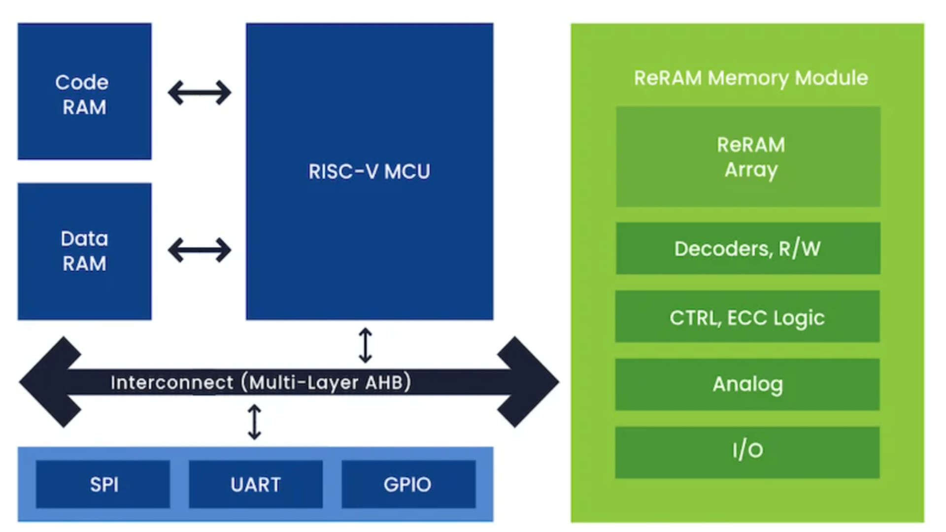
Weebit implements its ReRAM as a back-end-of-line module, allowing integration without modifying the front-end transistor structures.
This approach keeps incremental wafer costs at almost 5%, compared to the much higher overhead associated with integrated flash processes.
The memory cell itself relies on resistive switching instead of floating-gate storage, allowing bit-level access without block erase operations.
These design decisions are presented as pragmatic rather than revolutionary, relying on standard materials and conventional manufacturing tools.
“We said from day one that we would use standard materials, tools and flows,” he said. “We didn’t want to give the fabs any excuses not to work with us.”
Specs-wise, Weebit reports write speeds up to 100x faster than built-in flash, as well as endurance ranging from 100,000 to 1 million cycles.
The company reports that power consumption is lower due to lower operating voltages and direct access modes.
Its CEO bluntly states that “power, speed, endurance, temperature and cost, on all the important axes for embedded memory, ReRAM is better than Flash”.
The company also emphasizes immunity to electromagnetic interference, contrasting its technology with MRAM.
“We have seen cases where magnetic fields have corrupted MRAM in consumer environments,” Hanoch said, adding that large manufacturers considered this risk unacceptable.
As process nodes shrink below 28nm, onboard flash becomes increasingly difficult to scale reliably.
Designers often compensate by pairing logic chips with external flash and transferring data to SRAM at startup, which increases complexity and power consumption.
Hanoch says non-volatile ReRAM removes this inefficiency, allowing for instant booting and tighter security limits.
The greater density of ReRAM compared to SRAM allows edge devices to store more data on the chip, directly improving the accuracy of calculations.
“More bits on the same silicon means better accuracy for inference,” he said, while also pointing to demonstrated neuromorphic experiments in which “the ReRAM bit behaves like a synapse.”
Weebit cites industry predictions that ReRAM revenue will grow about 45% annually, potentially reaching $1.7 billion within six years.
But its revenue remains modest, although growing, and the company attributes its slowing adoption to institutional caution rather than technical shortcomings.
“The biggest obstacle is human nature,” Hanoch said, while emphasizing silicon’s work on multiple nodes and the qualifications for mass production.
It remains to be seen whether TI’s endorsement confirms that “ReRAM is the replacement for flash.”
However, the quest for universal memory remains uncertain, with alternatives such as ULTRARAM, developed by Quinas Technology, entering the field last year.
Follow TechRadar on Google News And add us as your favorite source to get our news, reviews and expert opinions in your feeds. Make sure to click the Follow button!
And of course you can too follow TechRadar on TikTok for news, reviews, unboxings in video form and receive regular updates from us on WhatsApp Also.