- Photonic fleas with quantum lasers are finally under construction without rethinking the entire system
- These lasers work directly on silicon and always survive high heat for more than six years
- Researchers from the University of California have filled the laser gap with polymers and control of the precision beam nailed to the chip
A new manufacturing method could make photonic circuits cheaper and more practical by directly incorporating quantumly lasers (QD) on silicon chips, a process that could influence the way future intelligent house devices, fitness trackers and even portable computers are designed.
The research team, led by Rosalyn Kosca at the University of California, succeeded by combining three key strategies.
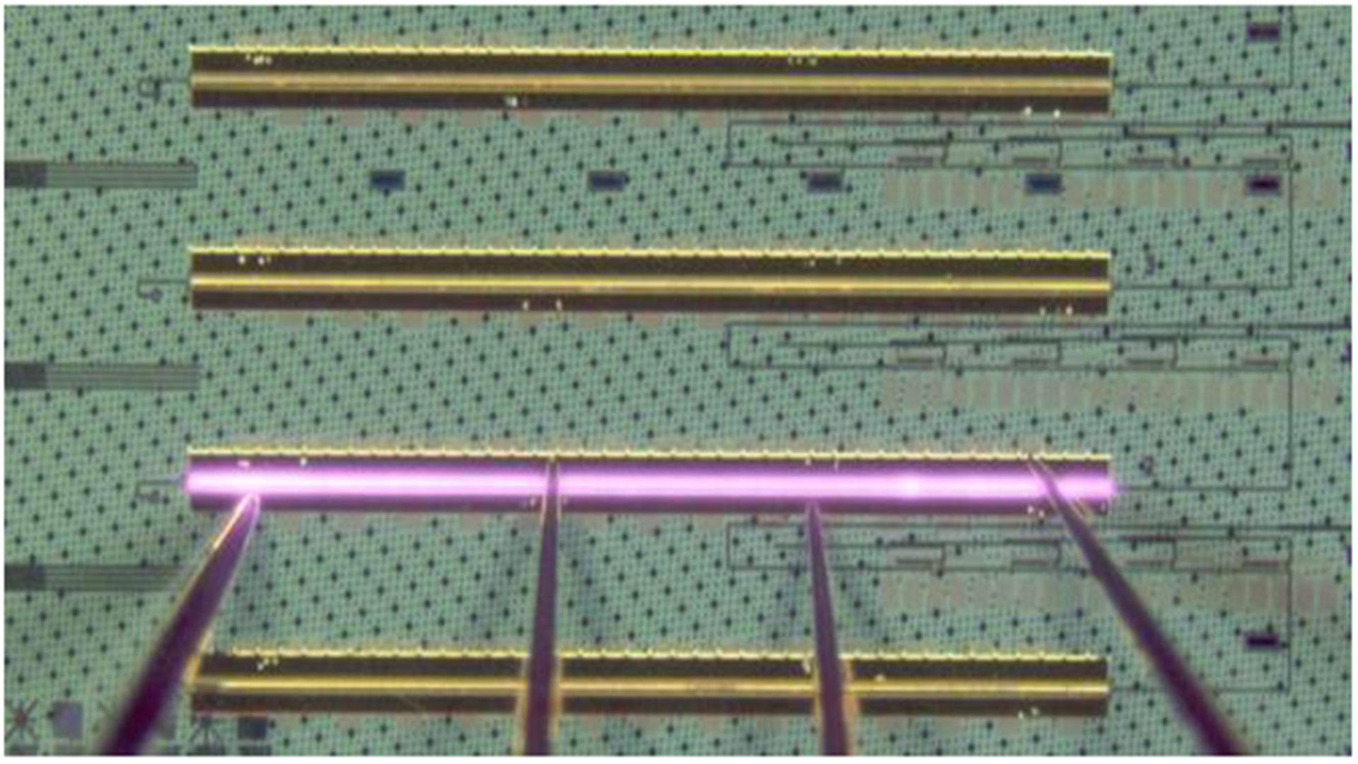
They used a pocket laser configuration for direct integration, followed a two-step growth method involving the deposit of metal-organic chemical steam and the epitaxy of the molecular beam, and introduced a technique for filling polymer space to reduce the propagation of the optical beam.
Go around the gap with meticulous engineering
This development is a long -standing challenges involving material incompatibilities and coupling ineffectiveness which have historically limited the performance and scalability of integrated photonic systems.
The combined efforts have minimized the initial interface gap and allowed the lasers to operate reliably on silicon photonic chiplets.
As the researchers note, “the integrated photonic circuit applications (PIC) require lighting sources on a chip with a small device imprint to allow the integration of denser components.”
The new approach allows stable monomod lasage at the O-Bande frequency, which is well suited to data communications in data centers and cloud storage systems.
By integrating lasers directly with silicon rings resonators or using Bragg reflectors distributed from silicon nitride, the team also addressed problems related to alignment and optical feedback.
One of the most surprising discoveries of research is the way lasers work under the heat.
“Our integrated QD lasers have demonstrated a high temperature lasier up to 105 ° C and a lifespan of 6.2 years while operating at a temperature of 35 ° C,” explains Ms. Kosca.
These performance measures suggest a level of thermal stability previously difficult to achieve with monolithically integrated conceptions.
This thermal resilience opens the door to more sustainable applications in real environments, where temperature fluctuations can limit the reliability of photonic components.
This can also reduce the need for active cooling, which has traditionally added the cost and complexity to past conceptions.
Beyond the performance, the integration method seems well suited to large-scale manufacturing.
Since the technique can be executed in standard semiconductor foundries and does not require major modifications to the architecture of underlying chips, it is promising for wider adoption.
Researchers argue that the method is “profitable” and “can work for a range of integrated photonic flea designs without the need for extensive or complex modifications”.
That said, the approach will probably face a meticulous examination concerning consistency in large sections and compatibility with commercial photonic systems.
In addition, success in controlled laboratory environments does not guarantee transparent deployment in mass manufacturing parameters.
However, the combination of a compact laser design, compatibility with conventional processes and the integration of O-Band functionality makes this development notable.
From data centers to advanced sensors, this laser integration compatible with silicon could bring the photonic circuits closer to the viability of the Masse market.
Via ieee