- Researchers have created a NAND-DRAM hybrid, inspired by existing camera technology
- Zinc Indium Gallium Oxide Also Promises Benefits Over Silicon
- For now, it’s just a prototype that requires further work.
Belgian semiconductor research center imec has unveiled what it claims to be the first 3D implementation of a charge-coupled device (CCD) memory architecture, which revives a technology already used in digital cameras and camcorders, but for an entirely different purpose.
Using the 3D CCD architecture, researchers were able to eliminate one of the biggest bottlenecks in AI computing today – the memory wall – where GPUs and accelerators spend more time waiting for data than processing it due to poor memory bandwidth and power efficiency.
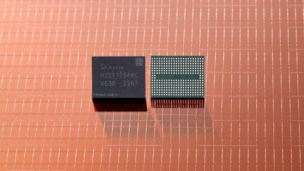
The new design combines the speed and rewrite of DRAM with the density and efficiency of NAND to form a type of hybrid.
Old camera technology could actually lead to future generations of memory
CCD technology is nothing new: charge-coupled devices have long been used in digital cameras, broadcast video equipment, scientific imaging, and even astronomy sensors, but CCDs have since been replaced by CMOS image sensors.
Traditionally, CCDs work by physically moving electrical charges between semiconductor gates, and this same principle applies to Imec’s research to enable highly efficient memory movement.
Instead of arranging memory cells side-by-side on a flat plane, like conventional DRAM, the design stacks them vertically in a sense similar to 3D NAND, which is important because DRAM’s limitations include leakage, higher manufacturing costs, and a reduction in the speed with which density improvements occur.
The chips also replace silicon with IGZO (Indium Gallium Zinc Oxide), which promises less leakage, longer data retention, easier low-temperature processing, and strong compatibility with dense 3D stacking.
With this hybrid architecture, imec has already demonstrated successful charge transfer at transfer speeds above 4 MHz, but this is still a very early stage technology and the prototype uses only a small number of stacked layers. In theory, it should be able to scale as well as NAND, with commercial chips now exceeding 200 layers.
The CCD architecture appears to promise reduced wear mechanisms and endurance that could even exceed NAND, making it ideal for very intensive applications on AI training clusters and inference servers.
“Unlike byte-addressable DRAM, our 3D CCD device is designed to provide block-level data access, which is better suited for modern AI workloads,” added Maarten Rosmeulen, program director for storage memory.
“The potential of this CCD device for use as a buffer lies in its ability to be integrated into a 3D NAND Flash chain architecture – the most cost-effective way to achieve high, scalable bit density, estimated well beyond the limit of DRAM. »
The research also details future plans for the promising architecture, positioning it as a CXL Type-3, or industry-standard, device for connecting GPUs, CPUs, and accelerators. This is an important consideration, with hyperscalers now turning to CXL as AI models become too large for local GPUs alone.
As a prototype and research product, there are still many hurdles to overcome, including thermal behavior, scaling the number of layers, and of course real-world integration. However, if successful, the new hybrid architecture could seriously help reduce one of the biggest costs of AI infrastructure, DRAM.
Looking ahead, imec proposes that the next phase may involve an entirely new class of memory architecture rather than simply evolving existing designs.
![]()
Follow TechRadar on Google News And add us as your favorite source to get our news, reviews and expert opinions in your feeds.