
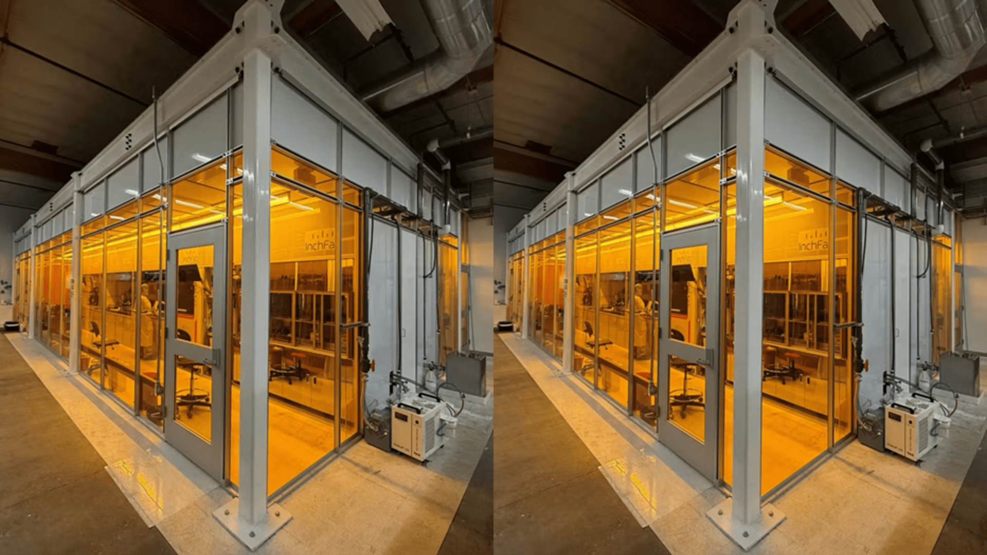
- Small wafer fabs could significantly reduce semiconductor manufacturing startup costs worldwide
- Compact chip factories could accelerate semiconductor workforce training in developing sectors
- InchFab believes utilization matters more than wafer size in semiconductor economics
The semiconductor industry has traditionally depended on massive manufacturing plants costing billions of dollars and requiring years to even begin significant chip production.
A US start-up called InchFab believes that much smaller facilities could significantly reduce these barriers by downsizing semiconductor manufacturing equipment themselves.
Founded by MIT graduate Mitchell Hsing, along with several collaborators, the company builds compact cleanroom manufacturing systems designed around smaller silicon wafers.

Smaller wafers reduce manufacturing costs
Instead of building vast industrial campuses processing huge volumes of wafers, InchFab compresses manufacturing capacity into modular systems roughly matching the dimensions of shipping containers.
The company says these systems cost between $5 million and $15 million, well below conventional semiconductor manufacturing facilities requiring multibillion-dollar investments.
Hsing explained that the company initially experimented with one-inch wafers because standard photolithography fields naturally aligned with these physical dimensions.
This approach quickly ran into practical complications, because one-inch wafers are difficult to find commercially and require manual cutting from larger substrates.
It then evolved into two-inch wafers before finally settling around four-inch formats that balanced practicality and the benefits of equipment miniaturization.
According to Hsing, shrinking manufacturing systems changes the physics surrounding plasma processing, as the surface area of the chamber becomes more and more dominant compared to the internal volume.
He noted that plasma-based systems contain layers of protective sheathing that prevent the chamber walls from degrading during operation.
Some engineering challenges appear to become easier in smaller dimensions, as pumps, valves, mass flow controllers, and vacuum control systems require smaller operating volumes.
Hsing said controlling compact plasma chambers simplifies several back-end processes compared to maintaining stability inside large semiconductor industrial equipment operating continuously at scale.
Compact FABs support multiple techniques
InchFab says its systems still perform many standard semiconductor manufacturing processes used in established manufacturing environments around the world.
The company lists lithography, metrology, plasma-assisted deposition, atomic layer deposition, dry etching, and several wet processing techniques among the supported manufacturing capabilities.
Hsing acknowledged that lithography remains the company’s main limitation, as element size and production speed still depend heavily on exposure technology constraints.
He explained that electron beam methods can theoretically achieve extremely small geometries, although slower write speeds reduce practicality for large manufacturing volumes.
Critics question whether small wafers can remain economically competitive with large manufacturing plants processing thousands of wafers each month on an industrial scale.
Hsing directly rejected this criticism, saying that the economics of manufacturing depend more on utilization rates and capital efficiency than on wafer dimensions alone.
“Today, we can often be price competitive with an 8-inch foundry,” Hsing said in discussing specialized requirements for industrial and aerospace manufacturing.
The company currently serves customers operating in the biomedical, sensing, aerospace, defense, photonics and compound semiconductor industries.
All of these areas require low production volumes and custom process flows tailored to InchFab.
InchFab’s business also involves workforce training for countries trying to establish domestic semiconductor manufacturing capacity without waiting years for large facilities.
“There is no better, no less expensive way to get started than with something like an InchFab,” Hsing said when discussing workforce development programs.
It remains to be seen whether compact factories truly democratize semiconductor manufacturing.
Advanced chip production still relies heavily on lithography performance and manufacturing consistency.
Nonetheless, smaller manufacturing systems could become increasingly attractive to specialized industries where flexibility, training and reduced capital matter more than scale.
Via IEEE spectrum

Follow TechRadar on Google News And add us as your favorite source to get our news, reviews and expert opinions in your feeds.